

The Holographic Metasurface Nano-Lithography (HMNL) process developed by my lab uses sub-wavelength-patterned metasurface masks (metamasks) to create multi-colored holograms in photocurable metal-polymer hybrid resins. This process allows entire 3D, multi-material (insulators and conductors) nanostructures to be patterned using a single light exposure. Metasurfaces can be encoded with much higher information density than traditional spatial light modulators such as digital micromirror devices, so the use of metasurface optics in HMNL overcomes many of the low-resolution and small-patterning-area challenges presented by conventional holographic 3D printing approaches. Additionally, the size of the hologram produced is limited only by the size of the fabricated metasurface. Using this method, we have demonstrated the ability to fabricate structures with ~500 nm resolution over areas greater than 30 mm × 30 mm. We have also demonstrated that metasurface optics can be designed to produce different holographic patterns when exposed to different colors of light and have developed a new resin chemistry that produces conductive metal structures when exposed to UV light and dielectric polymer insulators when exposed to visible light. By combining these two advances, we can build 3D metal-insulator composite structures at a rate of over 20 mm3/s.
You are here
Projects
Current Projects
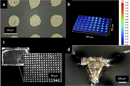
Additive manufacturing is well suited to making complex structures, but unfortunately current commercially available metal additive-manufacturing tools have feature-size resolutions of > 100 μm, which is too large for microelectronic interconnects. Research-grade metal additive manufacturing tools do exist, but their build rates are generally too slow for commercial applications. Therefore, the goal of the additive manufacturing work at the NDML is to improve the minimum feature-size resolution of metal additively-manufactured parts by up to two orders-of-magnitude, while still maintaining the throughput of traditional additive manufacturing processes. In order to achieve this goal, the NDML has developed a new microscale selective laser sintering system (μ-SLS) that uses micromirrors, high-speed nanopositioning stages, and a complex optical design to achieve write speeds on the order of 300 mm/s, and a feature-size resolution of ~ 1 μm. In this system, a laser is coupled to a fiber optic lens and directed off a micro-mirror array through a set of focusing objectives. This allows each 7.6 μm by 7.6 μm pixel in the micromirror array to be focused down to a spot size of approximately 1 μm. The μ-SLS also replaces the microscale powders used in conventional SLS processes with a nanoparticle (NP) ink. The use of NP ink in the μ-SLS system is required to build layers that are approximately 1 μm thick, because it is necessary to use particles that are at least one order-of-...
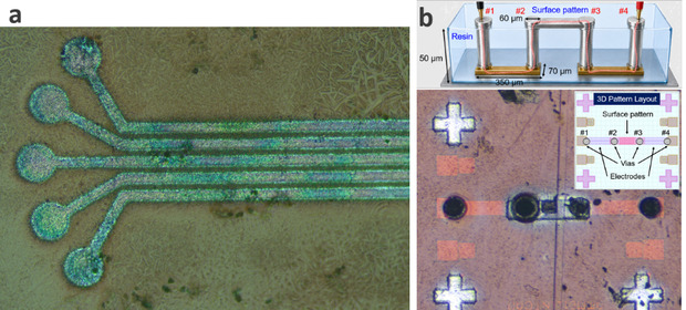
Advanced electronic packages need fine-pitch metal wiring embedded in a dielectric, which today is built up through many sequential lithography, plating and lamination steps. The NDML is developing a light-based additive process that prints conductors and insulators at the same time from a single resin. The resin combines metal salts with photopolymers, so the dose and wavelength of light at each voxel decide whether that region cures into a dielectric or forms a conductive silver network. Using patterned and holographic exposures, we can write redistribution layers, vias and interconnects in three dimensions without exchanging resins or making multiple passes. This work is part of the DARPA-funded Holographic Metasurface Nano-Lithography (HMNL) program with the University of Utah and industry partners, and aims to cut the time needed to build a custom package from months to days.
The figure above shows (a) printed silver lines and (b) a three-dimensional daisy chain with vertical vias printed through 50 μm of resin.
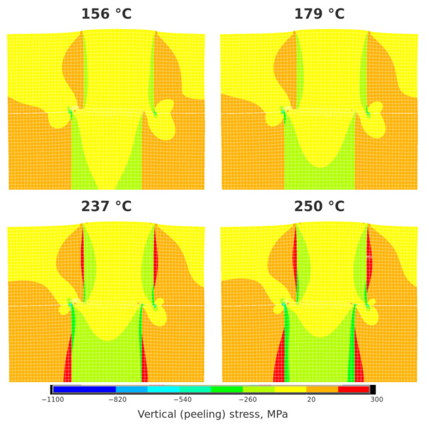
Hybrid bonding joins copper pads and oxide surfaces directly, enabling interconnect pitches of a few microns and below. However, the bond forms at a buried interface that cannot be inspected until after anneal, and failures are costly and irreversible. The NDML is building a digital twin that predicts bond quality before dies are joined. Pre-bond metrology such as AFM topography and copper dishing profiles sets the starting conditions for a set of linked simulations: molecular dynamics of the oxide–oxide and copper–copper interfaces, phase-field models of void closure and grain growth during anneal, and finite element models of die-scale stress and alignment. Machine-learned surrogates of these models are calibrated against test-vehicle data to create a virtual metrology layer that can guide process decisions as wafers move through the line.
The figure above shows a finite element model of a Cu–SiO2 hybrid bond with a 20% copper pad misalignment, with vertical (peeling) stress building at the Cu–SiO2 transition corners as the anneal ramps from 156 °C to 250 °C.
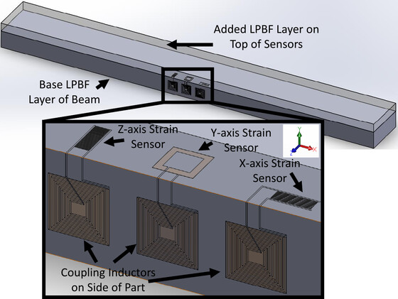
Fatigue-critical metal structures such as ship hulls, propellers, rotor blades and aircraft wings would benefit from sensors built directly into the load-bearing material. Through the DARPA SENSE program, the NDML and collaborators at UT Austin are developing a hybrid manufacturing process that embeds wireless strain and temperature sensors inside metal parts made by laser powder bed fusion. The build is paused so that a custom micro-cold spray system can deposit ceramic insulating films and metal traces into a cavity, forming a chipless RFID sensor from a printed coil and interdigitated capacitors. Printing then resumes to seal the sensor inside the part. Strain shifts the resonant frequency of the sensor and temperature changes its quality factor, so each sensor can be read wirelessly through an external coil. Simulations showed a temperature resolution of 0.4 °C and a strain resolution of 1.75×10⁻⁵, and complete parts with embedded sensors have been fabricated and tested.
The figure above shows the concept for a beam with embedded x-, y- and z-axis strain sensors read through coupling inductors on the side of the part.
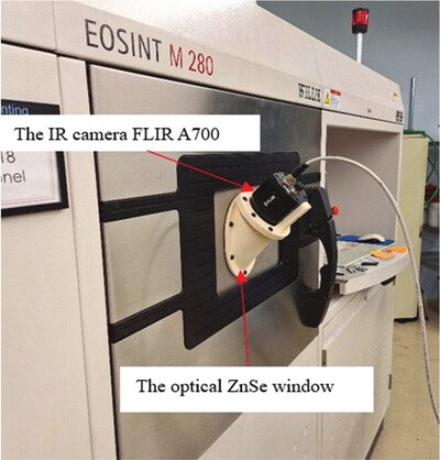
In laser powder bed fusion, melt pools that run too cold cause lack of fusion, while melt pools that run too hot cause evaporation and porosity. The NDML is developing infrared thermography methods that measure melt-track temperatures during the build with quantified uncertainty. An infrared camera mounted at the optical window of an EOSINT M280 records each layer, and Kalman filtering combined with measured powder emissivity converts the images into temperature estimates with an uncertainty of about ±7%. These measurements sort each region of the build into quality classes and can be used to generate control signals that adjust the laser power. The approach has been demonstrated on 316L stainless steel and Inconel 718, including studies of how powder particle size affects melt pool stability and porosity.
The figure above shows the infrared camera installed on the EOSINT M280.
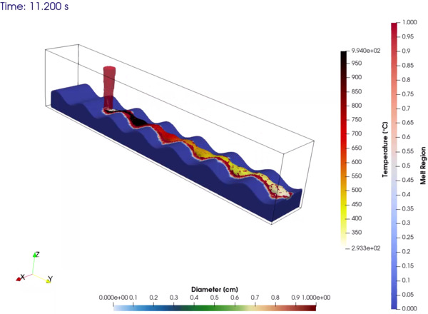
Directed energy deposition (DED) is widely used to build and repair large metal parts for aerospace, automotive and tooling applications, but the height and shape of each deposited layer drift as the melt pool responds to changes in the part below it. In collaboration with Missouri University of Science and Technology, the NDML uses multiphysics simulations of Inconel 718 deposition to understand these dynamics. The models capture multiphase flow, heat transfer, solidification, surface tension and Marangoni effects, and are used to study how laser power, scan speed, standoff distance and substrate geometry affect melt pool size and deposit height. Current work drives the process with sinusoidal substrate disturbances to measure its frequency response, which will form the basis for a model-based height controller.
The figure above shows a simulated deposition track over a wavy substrate.
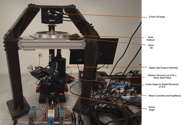
Large telescope and satellite mirrors are expensive and slow to make because they require extensive grinding and polishing. The NDML is developing a projection micro-stereolithography system that prints optical surfaces directly. The system uses an r–θ motion architecture, in which a rotary stage and a radial linear stage move a digital light engine beneath the resin vat, so that a small, high-resolution projection field can cover a build area much larger than the field itself. Replacing the polymer film at the bottom of the vat with a rigid quartz constraint surface reduced the printed surface roughness from several microns to tens of nanometers. The goal of this work, carried out in collaboration with Triton Systems, is a scalable process for printing large-diameter optics with nanometer-scale surface finish.
The figure above shows the completed r–θ printing system.
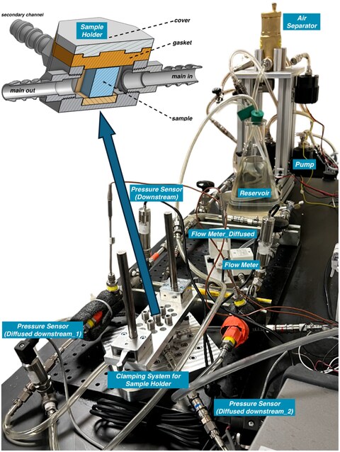
Recovering critical elements such as cobalt, nickel and lithium from batteries and industrial waste requires sorbents that combine a large surface area with fast flow. The NDML uses digital light processing to print gyroid structures with pores at two length scales: the gyroid geometry provides open millimeter-scale channels for flow, while polymerization-induced phase separation creates nanometer-scale pores within the walls. By changing the porogen mix in the resin and the wall thickness, we can trade off diffusion rate against mechanical strength. Receptor molecules bound into the porous walls allow selective capture and fast release of target metals, and the printed cartridges fit into a modular flow platform that can be reconfigured for different separations.
The figure above shows the flow test system used to measure pressure drop and diffusion through the printed gyroids (from Gao et al., Advanced Engineering Materials, 2026, CC BY-NC-ND 4.0).
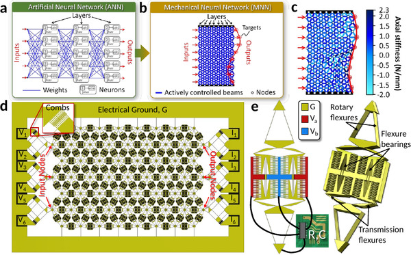
Mechanical neural networks (MNNs) are architected materials that learn behaviors by tuning the stiffness of their beams, in the same way that artificial neural networks tune their weights. In collaboration with Prof. Jonathan Hopkins at UCLA, the NDML is scaling MNNs down from tabletop prototypes to microfabricated lattices. We have built meso-scale MNN lattices in which each beam contains MEMS thermal actuators and piezoresistive sensors under closed-loop control, allowing each beam to reach a programmed positive or negative stiffness within hundreds of milliseconds. Current work uses electrostatic comb-drive actuators and co-designed control electronics to push MNN response speeds toward the limits set by the material itself, for applications such as ultra-precision motion stages and adaptive structures.
The figure above shows how an MNN maps onto an artificial neural network, along with a comb-drive MNN lattice design.
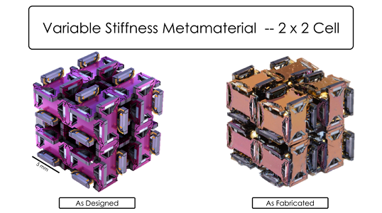
One new project in the NDML is the design, fabrication, and assembly of novel MEMS devices to create mechanical metamaterials with programmable stiffnesses. The MEMS devices used in this project are designed to have unique bidirectional thermal actuators which are capable of outputting large amounts of force in both tension and compression. The bidirectional MEMS actuators contain two actuating components, the inner actuator and outer actuator, both contained within an out-most enclosure. The outer actuator consists of a pair of multi-chevron beam structures mirrored and connected at the anchor and the inner actuator is a set of horizontal beams connecting the anchors through the handle layer. When a voltage is applied across the black electrodes, current flows through the outer actuator and the chevron beams undergo joule heating and thermal expansion. The outward horizontal motion at the anchors are restricted by the inner actuator beams, resulting in an upwards displacement at the tip of the device. Conversely, when a voltage is applied across the white electrodes, current flows through the center beams. The thermally expanded beams push the anchors outwards which results in a downwards displacement at the tip of the device. The MEMS devices also have piezoresistive strain sensors which are capable of very sensitive displacement measurements. Therefore, when the MEMS devices are assembled into a cube, they are capable of measuring an input force applied to the cube and then...
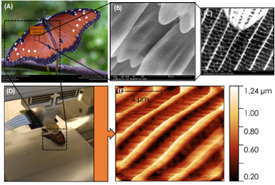
Through the application of compact, MEMS-based single chip atomic force microscopes (sc-AFMs) with high scanning speeds, we have developed a R2R metrology tool that greatly increases the throughput and modularity of direct, nanometer-scale measurement on flexible substrates. Designed to provide feedback for a R2R nanopatterning applications, the proof-of-concept system consists of a simple three roller unwind-idler-rewind web-handling arrangement, with the idler roller supported by radial air bearings to enable sensitive, on-roller measurements of the polycarbonate web. Two voice-coil driven vertical, double parallelogram flexure mechanisms are used to precisely position a gantry that holds the sc-AFM probe over the idler roller for web inspection. The nanopositioning sub-system quickly brings the sc-AFM probe within its 20 µm scanning height envelope on startup and rejects any external disturbances that could cause destructive tip-web contact. The probe is held at ideal scanning height for in-line measurement by compensating for idler roller eccentricity and topology using an offline map. Overall, this R2R nanometrology concept is highly scalable due to the modular nature of the fine-approach mechanism, sc-AFM sub-system, and parallelized, discrete control of each individual sc-AFM. We have also recently demonstrated that this system is capable of achieving sub-1 nm vertical resolution, 16.6 nm lateral resolution, and a throughput of 400 μm2/min with a web speed up to 2...
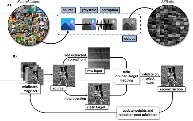
Atomic force microscopy (AFM) provides nanometer-scale topography, but high-quality scans are slow and require careful manual post-processing, which limits the use of AFM for in-line metrology. In collaboration with Sandia National Laboratories, the NDML has developed machine learning methods that reconstruct high-resolution images from fast, noisy scans. Our first approach used a Noise2Noise-style U-Net to recover the quality of slow scans from data taken nearly three times faster. Building on this, AFM-net trains on large sets of natural images corrupted with artifacts extracted from real AFM data. This overcomes the scarcity of AFM training data and lets a single model correct line noise, tilt and scars while predicting feature heights. The approach processes each scan in seconds rather than minutes and also generalizes to scanning tunneling microscope images.
The figure above shows the AFM-net training workflow.
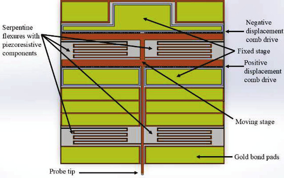
Interfacial forces govern adhesion, friction and chemical bonding at the nanoscale, but conventional atomic force microscopes suffer from a snap-to-contact instability that hides much of the force–distance curve. The NDML is developing a MEMS-based interfacial force microscope that removes this instability through force feedback. The silicon device suspends a probe on serpentine flexures with integrated piezoresistive sensors, while electrostatic comb drives apply a counteracting force so that the probe stays at zero displacement. This allows the instrument to measure the full interaction force as the tip approaches and retracts from a surface. The first experiments will measure the strength of single reversible covalent bonds to guide the design of tougher, more sustainable polymers.
The figure above shows the layout of the device.
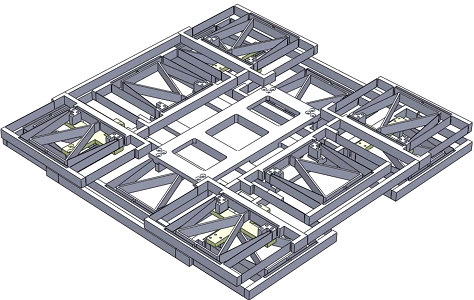
Long-range nanopositioning is a key enabling technology, catalyzing advances in a variety of existing and emerging domains such as scanning probe microscopy, semiconductor packaging and inspection, high-density data storage, micro additive manufacturing, and nano-metrology. Flexure bearings have emerged as a ubiquitous choice for nano-positioning applications since they experience low hysteresis and eliminate the effects of friction and backlash. The conflicting requirements of centimeter scale travel, high bandwidth, low stress concentration, and adequate safety factor make it challenging to design a compact flexure-based positioning stage. Existing designs demonstrate high accuracy and resolution, but acknowledge that large motion ranges are achieved at the cost of low resonant frequency.
The purpose of this research is to enable high-speed, long-range nanopositioning through computational optimization of Double Parallelogram (DP) flexure-based nanopositioning stages. The proposed methods can be used to design a platform with two degrees-of-freedom, meeting the required static and dynamic performance characteristics in a compact form-factor. By stacking planar DP units with optimized structural members, the proposed design can travel 50 mm in each axis with sub...
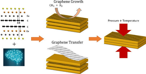
Copper is the standard conductor for power and signal wiring, but its resistance rises with temperature and it oxidizes in harsh environments. With support from NASA, the NDML is developing copper–graphene composite conductors for high-voltage power transmission in space. The work pairs atomistic simulation and machine learning to design the composite with experiments that grow or transfer graphene onto thin copper films and foils, consolidate the layers under heat and pressure, and draw them into wire. Our simulations showed that compressive strain, rather than graphene doping alone, is what raises the conductivity of copper. Multilayer copper–graphene films showed a lower temperature coefficient of resistance, a 61% higher oxidation failure temperature and higher current-carrying capacity than pure copper, and graphene-coated foils have been drawn into wires.
The figure above shows the design and fabrication approach.
Past Projects

One type of device that is of particular interest to the NDML is graphene-based nanoelectromechanical resonators (GNEMS). This is because GNEMS can be used as both extremely sensitive mass/force detectors for biosensing applications and as highly tunable, reconfigurable electromechanical filters for communications applications. GNEMS resonators offer the potential to overcome many of the limitations of traditional MEMS-based resonators because of graphene’s outstanding electrical and mechanical properties. For example, graphene has an extremely high stiffness-to-weight ratio, which makes it possible to construct graphene resonators with very high natural frequencies. Also, graphene has a very high yield strain, which allows it to be stretched to very large tensions before failure. These properties allow us to tune the resonance frequency of a single graphene resonator over an extremely wide range (~ three orders of magnitude from MHz to GHz), which is important in communications and sensing applications.
One of the major challenges in producing highly accurate graphene-based sensors and filters is the poor fabrication repeatability of graphene resonators due to small variations in the residual stress and initial tension of the graphene film. This has meant that graphene-based nanoelectromechanical resonators tend to have large variations in natural frequency and quality factor from device to device. This poor repeatability makes...
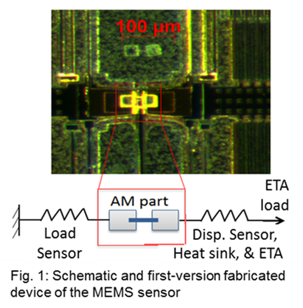
New polymer-based additive manufacturing (AM) systems have recently been developed that use 2-photon lithography to write 3-dimensional features with a resolution of approximately 200 nm. However, little is known about how processing parameters or the uncured polymer formulation effect the mechanical properties of the printed nanoscale structures. Therefore, we have developed a MEMS-based mechanical testing system onto which nano-AM structures can be printed in order to directly measure the mechanical properties of the 3D printed polymer structures. In this system, the nano-AM specimen is printed so that it is suspended between two MEMS stages. Each MEMS stage is connected to a set of capacitive sensors in order to be able to measure the displacement of each stage during testing. A thermal actuator is used to pull on one of the stages and to apply strain to the printed polymer sample. A capacitive sensor attached to the second stage is used to measure the total force applied to the sample. For precise and accurate characterization of a variety of print parameters, two different tensile testers have been created, one with a fine displacement resolution of 0.25 nm and the other with a high load capacity of 25 mN. Thus, this tensile tester can be used to generate the force-displacement curves for a wide verity of printed features, thereby enabling the characterization of the mechanical properties of nano-AM structures with unprecedented precision. This is a critical advance in our...
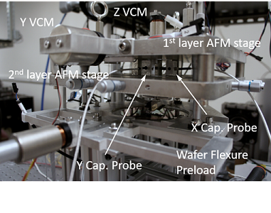
Atomic force microscopy is capable of producing very high resolution (sub-nm-scale) surface topology measurements and is widely utilized in scientific and industrial applications, but has not been implemented in-line with manufacturing systems, primarily because of the large setup time typically required to take an AFM measurement. In order to overcome this limitation, the NDML has developed a single-chip-AFM-based inspection system where a wafer can be precisely and repeatably loaded into the setup and measurements can be taken in under 60 seconds.
This inspection system consists of several single-chip AFMs integrated into a positioning stage to make measurements at multiple spots on a wafer at the same time, as shown in Figure 6. Each single-chip AFM is a MEMS device that is approximately 2 mm wide by 1 mm tall and is capable of scanning a 10 μm by 10 μm area. Thermal actuators in the MEMS device are used to do the scanning in both the x and y directions as well as to excite the z axis of the AFM so that it can be run in taping mode. Each AFM is attached to a flexure stage in the top plate of the inspection system so that the AFM can be precisely moved to the desired inspection location on the wafer. The flexure plate is coupled to the inspection plate using a kinematic coupling so that the flexure plate can be precisely located with respect to the inspection plate after each loading operation. In order to take a measurement, the...
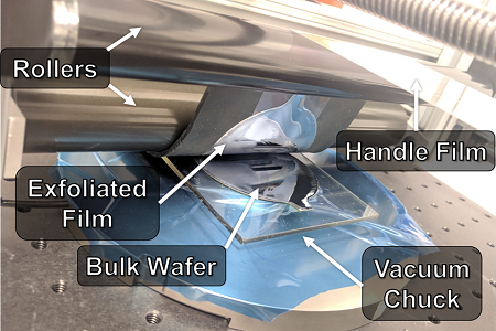
Single crystal silicon thin-films are extremely useful in a variety of applications where a combination of flexibility and high electronic performance is desired. The silicon exfoliation process is very cost-effective in creating thin-film Si compared with alternative methods such as etching or mechanical grinding. In the silicon exfoliation process nanoelectronic devices are first fabricated on a standard silicon wafer. A nitride passivation layer is then grown on top of the nanoelectronic devices, and a nickel layer is electroplated on top of the nitride in order to apply compressive stress to the silicon. This stress initiates a crack approximately 10 µm below the top surface of the silicon wafer, which can then be propagated along the wafer to produce a uniform, 10 µm thick, extremely flexible, single-crystal silicon film. To better control the exfoliation process, we developed an FEA-based fracture mechanics model which showed that by changing the angle of the applied load we could skew the mode mix ratio and, therefore, change the characteristic crack depth. Using this model, we designed a repeatable peeling tool that is capable of applying a constant exfoliation angle and force to the wafer during exfoliation. The tool features a simple, adjustable roller design attached to a linear actuator. The two-roller design moves a film over the wafer while maintaining a constant peeling angle and force. Testing has shown that by changing the tension in the...
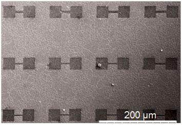
Most graphene-based NEMS devices are fabricated in a “one-off” manner using slow, limited scale methods such as mechanical exfoliation, electron beam lithography, or transfer from copper foils which can’t be incorporated into standard micro- and nanofabrication lines. In order to overcome this limitation, a method was developed that can be used to manufacture graphene-based NEMS devices at the wafer scale using conventional microfabrication techniques. In this project graphene is grown directly on thin film copper using chemical vapor deposition. The copper film is then patterned and etched to produce graphene-based NEMS resonators. This research is still in the early stages of development but this manufacturing method offers the potential to increase the throughput, yield, and repeatability of manufacturing graphene resonators while reducing the manufacturing cost and complexity.
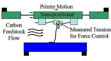
One of the greatest challenges in the development of nanoscale sensor systems and other nanomaterials-based devices is our inability to precisely, accurately, and repeatably place the desired nanomaterials and nanostructures where we want them, at a high rate and a low cost. For example, carbon nanotubes (CNTs) have long been seen as potentially transformative material due to their outstanding electrical (current density >109 A/cm2) and mechanical (elastic modulus > 1 TPa) properties. However, very few carbon nanotube-based devices exist due to our inability to manufacture CNTs at a large scale with the desired properties on any type of substrate. One potentially promising method for overcoming these is the direct printing of carbon nanotubes onto substrates. To achieve this type of direct printing, a chemical vapor deposition (CVD) furnace with integrated positioning and sensing to controllably grow and place CNTs onto a substrate is needed. This tip-based fabrication method would allow different types of nanotubes (single walled, multi-walled, functionalized, etc.) to be directly and precisely placed on prefabricated structures at a low cost and high speed.
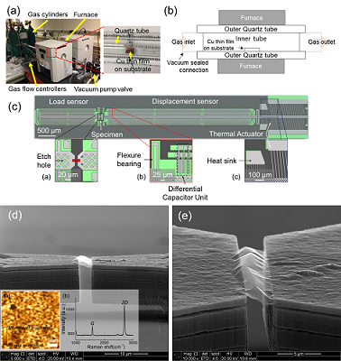
The goal of this research is to measure mechanical properties of graphene grown under different conditions which may affect the quality, grain sizes, and the number of layers of graphene. The mechanical properties of graphene are measured in many ways, yet conventional mechanical tensile testing of graphene sheets is difficult due to one atomic thickness of graphene and difficulties in handling graphene tensile specimen in nanoscale. We propose implementing Microelectromechanical System (MEMS) based tensile tester to accurately measure the mechanical properties of suspended graphene from strain versus stress curve.
Figures
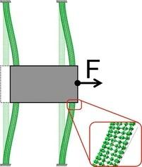
Carbon nanotubes (CNTs) may be used to create nanoscale compliant mechanisms that possess large ranges of motion relative to their device size. Many macroscale compliant mechanisms contain compliant elements that are subjected to fixed-clamped boundary conditions, indicating that they may be of value in nanoscale design. The combination of boundary conditions and large strains yield deformations at the tube ends and strain stiffening along the length of the tube, which are not observed in macroscale analogs. In this project molecular dynamics simulations are used to help model and design a nanoscale linear bearing system. These simulations show that the large-deflection behavior of a fixed-clamped CNT is not well-predicted by macroscale large-deflection beam bending models or truss models. However, pseudo-rigid-body modeling may be adapted to capture the strain stiffening behavior and, thereby, predict a CNT’s fixed-clamped behavior with less than 3% error from molecular simulations. The resulting pseudo-rigid-body model may be used to set initial design parameters for CNT-based compliant mechanisms. This removes the need for iterative, time-intensive molecular simulations during initial design phases.
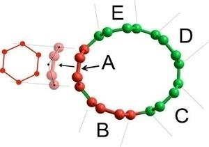
Molecular dynamics simulations can be used to examine the mechanical properties of carbon nanotubes when both axial and lateral forces are applied to the CNT. However, this project shows that an elastic tube model of a (5,5) carbon nanotube predicts stretching and bending moduli that differ by 19%. This is due to (1) differing energy storage mechanisms in each mode and (2) the inability of the tube model to capture these effects. Conventional tube models assume a common energy storage mechanism in stretching and bending. They show that energy is stored primarily through bond stretching/rotation and bond torsion/van der Waals interactions in stretching and bending, respectively. This knowledge underscores the need to use different moduli to predict stretching, bending, and combined bending and stretching when using the tube model.
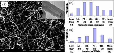
In this project a growth model was developed to control the diameter and number of walls in multi-walled carbon nanotubes grown by chemical vapor deposition (CVD). From this model, tunable process parameters may be used to control the geometry or stiffness of multi-walled carbon nanotubes (MWCNTs). This is important to devices that rely on the compliance of MWCNTs in order to achieve specific performance requirements, e.g. deflection or stiffness. Examples of these types of devices include relays, resonators and flexural bearings for small-scale actuators. It is necessary to control the stiffness of these mechanisms because the force, stroke, and device bandwidth depend upon the stiffness of the constituent MWCNTs. For a given length MWCNT, the stiffness is controlled by the MWCNT diameter and the number of walls in the MWCNT. The diameter and number of walls are controlled by adjusting several growth parameters – temperature, catalyst film thickness, and hydrocarbon concentration. Using thermodynamic relations, optimal growth parameters can be determined for CNTs with specific stiffnesses and natural frequencies. Overall, I was able to control the CNT geometry with less than 7 percent error and the stiffness and natural frequency with less than 2 percent error.
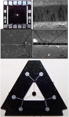
As mechanical devices move towards the nanoscale, smaller and more sensitive force and displacement sensors need to be developed. Currently, many biological, materials science, and nanomanufacturing applications could benefit from multi-axis micro- and nanoscale sensors with fine force and displacement resolutions. Unfortunately, such systems do not yet exist due to the limitations of traditional sensing techniques and fabrication procedures. Carbon nanotube-based (CNT) piezoresistive transducers offer the potential to overcome many of these limitations. Previous research has shown the potential for the use of CNTs in high resolution micro- and nanoscale sensing devices due to the high gauge factor and inherent size of CNTs. However, a better understanding of CNT-based piezoresistive sensors is needed in order to be able to design and engineer CNT-based sensor systems to take advantage of this potential. The purpose of this research is to take CNT-based strain sensors from the single element test structures that have been fabricated and turn them into precision sensor systems that can be used in micro- and nanoscale force and displacement transducers. In order to achieve this purpose and engineer high resolution CNT-based sensor systems, the design and manufacturing methods used to create CNT-based piezoresistive sensors were investigated. At the system level, a noise model was developed in order to be able to optimize the design of the sensor system. At the...
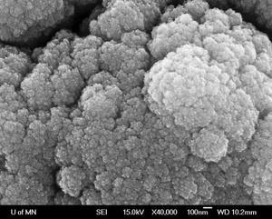
Si–Ti–N nanostructured coatings were synthesized by inertial impaction of nanoparticles using a process called hypersonic plasma particle deposition (HPPD). A study detailing the effect of plasma gases showed that in the case of an Ar+H2 plasma gas mixture, crystalline phases in the coatings consisted of TiN, TiSi2, and Ti5Si3. When the system was switched to a plasma gas mixture of Ar+N2, the only crystalline phase was TiN. Transmission electron microscopy confirmed the presence of TiN crystallites in an amorphous matrix. Warren–Averbach analysis indicated the average size of the TiN crystallites to be 14.9 nm. In separate experiments with the same conditions, aerodynamic lenses were used to deposit particles directly onto TEM grids. We observed agglomerated structures with an Ar+N2 plasma, while with an Ar+H2 plasma we found discrete TiSix and TiNx particles. In-situ particle diagnostics indicated only small changes in the particle size distributions when the plasma gases were changed.
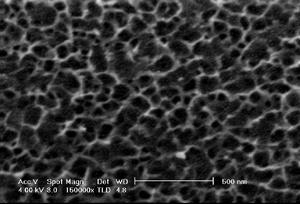
The excellent electrical and mechanical properties of porous nanostructured titania (NST) make it an ideal material for many different applications including dye sensitized solar cells (DSSC). While DSSCs are cheaper to manufacture than silicon-based cells, they are also less efficient. The efficiency of the DSSCs depends on how well the sensitizing dye coats the cell and how well the electron recombination source infiltrates into the porous NST. Consequently, the structure of the NST has a great effect on the efficiency of the cell. Different processing parameters were studied to determine their effects on pore size and surface area. Overall, it was found that increasing the deposition rate and the thickness of the original titanium film increased the pore size of the NST. Also, it was found that increasing the concentration of the hydrogen peroxide used to oxidize the titanium, increased the pore size of the NST. In general, it was also found that as pore size increased, surface area decreased.