
Advanced electronic packages need fine-pitch metal wiring embedded in a dielectric, which today is built up through many sequential lithography, plating and lamination steps. The NDML is developing a light-based additive process that prints conductors and insulators at the same time from a single resin. The resin combines metal salts with photopolymers, so the dose and wavelength of light at each voxel decide whether that region cures into a dielectric or forms a conductive silver network. Using patterned and holographic exposures, we can write redistribution layers, vias and interconnects in three dimensions without exchanging resins or making multiple passes. This work is part of the DARPA-funded Holographic Metasurface Nano-Lithography (HMNL) program with the University of Utah and industry partners, and aims to cut the time needed to build a custom package from months to days.
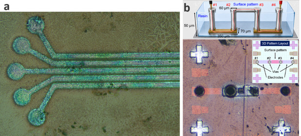
The figure above shows (a) printed silver lines and (b) a three-dimensional daisy chain with vertical vias printed through 50 μm of resin.