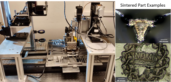
Advanced packaging now drives much of the progress in semiconductor performance. It needs interconnects and dielectrics patterned at scales and speeds that conventional lithography and plating struggle to reach. We develop additive processes that build these structures directly. Holographic metasurface nanolithography (HMNL) uses sub-wavelength metasurface masks to project multi-color holograms into a hybrid metal–polymer resin. This patterns entire 3D conductor–insulator structures with roughly 500 nm resolution in a single exposure.
-
-
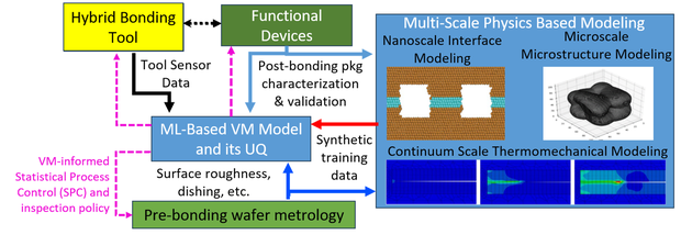
Hybrid bonding joins chips face to face through direct copper–copper and oxide–oxide bonds and is central to 3D heterogeneous integration. Bond quality, however, depends on nanometer-scale surface topography, material properties and process conditions that are hard to measure directly. We build multiscale simulations and digital twins of the Cu–SiO2 hybrid bonding process that link these inputs to bond formation, stress and yield.
-
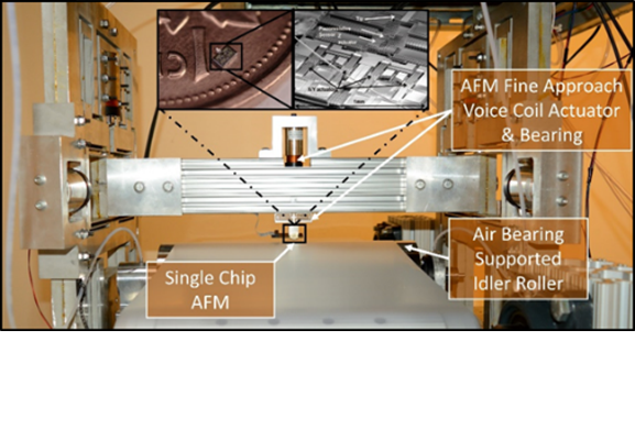
Scaling up nanomanufacturing requires measuring nanoscale features fast enough to control the process. We build in-line metrology systems and the data tools that make them practical. Our roll-to-roll inspection platform integrates MEMS-based atomic force microscopes into a moving web to measure nanopatterned films during production. Fast scans are noisy, so we develop machine-learning methods that reconstruct high-resolution topography from fast, sparse measurements and remove scan artifacts.
-
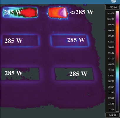
Metal additive manufacturing is only as reliable as our ability to see what happens in the melt pool and to quantify our confidence in each part. We use infrared thermography and synchronized in-situ measurements to monitor laser powder bed fusion of alloys such as 316L stainless steel and IN718. We have also developed methods to measure the emissivity of metal powders, so thermal images can be converted into accurate temperatures. Building on metrology principles, we apply statistical quality assessment and measurement-uncertainty analysis to judge whether a process is in control.
-
Many of our manufacturing and metrology advances depend on custom precision hardware. We design long-travel, flexure-based nanopositioning stages that combine centimeter-scale range with nanometer-level precision, and we add features such as eddy-current damping to improve their dynamics. At smaller scales, we build MEMS-based instruments for measuring forces and topography at the nanoscale, including a MEMS interfacial force microscope and single-chip atomic force microscopes.
-
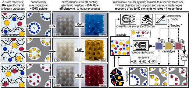
Additive manufacturing lets us design materials from the microstructure up. With collaborators in chemistry, we 3D print dual-scale gyroid structures whose nanoporous walls carry custom molecular receptors. These form modular cartridges that selectively capture critical elements from mixed streams. We also develop graphene–copper composite conductors that pair copper’s conductivity with improved thermal stability for aerospace power applications, and we study laser powder bed fusion of pure copper.
 The Nanoscale Design and Manufacturing Laboratory (NDML) at the University of Texas at Austin focuses on the design and development of novel processes and equipment for the manufacturing of micro and nanoscale devices and structures. As materials and mechanisms are scaled down to the nanoscale, new physical phenomena emerge, producing unique and extraordinary mechanical, electrical and thermal properties. However, taking advantage of these properties to create useful, marketable products has often proven difficult. These difficulties result from our inability to quickly and reliably incorporate nanostructures and nanoscale materials into micro/macroscale structures and devices. Therefore, new nanomanufacturing processes and equipment must be developed to overcome these limitations and enable the successful manufacturing of precise and repeatable nanoscale structures and devices for high-value defense, energy, and nanoelectronic applications. Current work in the NDML at UT-Austin focuses on several areas that are critical to the advancement of micro and nanomanufacturing including: