
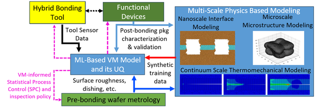
Hybrid bonding joins chips face to face through direct copper–copper and oxide–oxide bonds and is central to 3D heterogeneous integration. Bond quality, however, depends on nanometer-scale surface topography, material properties and process conditions that are hard to measure directly. We build multiscale simulations and digital twins of the Cu–SiO2 hybrid bonding process that link these inputs to bond formation, stress and yield. By combining physics-based models with machine-learning surrogates and in-line metrology data, these virtual metrology tools aim to predict bond quality before parts are bonded and to guide process decisions in advanced packaging manufacturing.