
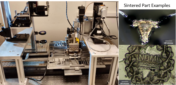
Advanced packaging now drives much of the progress in semiconductor performance. It needs interconnects and dielectrics patterned at scales and speeds that conventional lithography and plating struggle to reach. We develop additive processes that build these structures directly. Holographic metasurface nanolithography (HMNL) uses sub-wavelength metasurface masks to project multi-color holograms into a hybrid metal–polymer resin. This patterns entire 3D conductor–insulator structures with roughly 500 nm resolution in a single exposure. Microscale selective laser sintering (µ-SLS) uses a digital micromirror array to sinter copper nanoparticle films, writing micron-scale metal interconnects at high throughput. We also use two-photon photoreduction to write embedded 3D silver networks inside polymer dielectrics. Together these processes target redistribution layers, interconnects and heterogeneous integration for next-generation electronics packages.