Atomic force microscopy is capable of producing very high resolution (sub-nm-scale) surface topology measurements and is widely utilized in scientific and industrial applications, but has not been implemented in-line with manufacturing systems, primarily because of the large setup time typically required to take an AFM measurement. In order to overcome this limitation, the NDML has developed a single-chip-AFM-based inspection system where a wafer can be precisely and repeatably loaded into the setup and measurements can be taken in under 60 seconds.
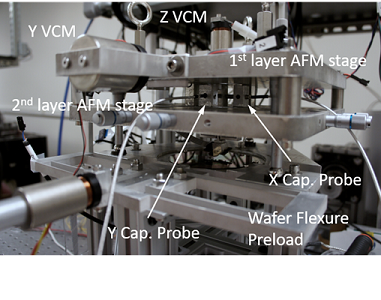
This inspection system consists of several single-chip AFMs integrated into a positioning stage to make measurements at multiple spots on a wafer at the same time, as shown in Figure 6. Each single-chip AFM is a MEMS device that is approximately 2 mm wide by 1 mm tall and is capable of scanning a 10 μm by 10 μm area. Thermal actuators in the MEMS device are used to do the scanning in both the x and y directions as well as to excite the z axis of the AFM so that it can be run in taping mode. Each AFM is attached to a flexure stage in the top plate of the inspection system so that the AFM can be precisely moved to the desired inspection location on the wafer. The flexure plate is coupled to the inspection plate using a kinematic coupling so that the flexure plate can be precisely located with respect to the inspection plate after each loading operation. In order to take a measurement, the flexure plate is removed from the inspection plate, a wafer is loaded into the inspection plate using an exactly constrained, passive alignment system, and the flexure plate is then placed back onto the inspection plate. This brings the AFMs back into contact with the surface that is to be measured and the AFMs can then start taking measurements without any additional alignment operations. The overall measurement procedure takes less than one minute, which is faster than most nanomanufacturing processes. This guarantees that the inspection step will not be the bottleneck in the manufacturing process. Overall, this system has been measured to have a vertical resolution of 0.48 nm and a lateral resolution of 1.64 nm which enables the measurement of even the smallest features typically found in the nanomanufacturing environment.