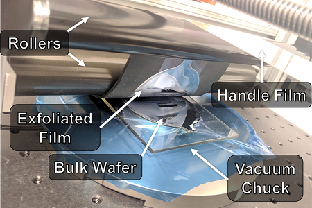
Single crystal silicon thin-films are extremely useful in a variety of applications where a combination of flexibility and high electronic performance is desired. The silicon exfoliation process is very cost-effective in creating thin-film Si compared with alternative methods such as etching or mechanical grinding. In the silicon exfoliation process nanoelectronic devices are first fabricated on a standard silicon wafer. A nitride passivation layer is then grown on top of the nanoelectronic devices, and a nickel layer is electroplated on top of the nitride in order to apply compressive stress to the silicon. This stress initiates a crack approximately 10 µm below the top surface of the silicon wafer, which can then be propagated along the wafer to produce a uniform, 10 µm thick, extremely flexible, single-crystal silicon film. To better control the exfoliation process, we developed an FEA-based fracture mechanics model which showed that by changing the angle of the applied load we could skew the mode mix ratio and, therefore, change the characteristic crack depth. Using this model, we designed a repeatable peeling tool that is capable of applying a constant exfoliation angle and force to the wafer during exfoliation. The tool features a simple, adjustable roller design attached to a linear actuator. The two-roller design moves a film over the wafer while maintaining a constant peeling angle and force. Testing has shown that by changing the tension in the peeling film we are able to precisely set and control our exfoliated film thickness from 5-25μm. The samples also show improvement in usable area per wafer and reductions in the surface roughness of the exfoliated samples.